
Specify a vision inspection system from the decision it must make: presence, orientation, dimension, defect or code. For an electronics line, the smallest relevant feature, surface reflectivity and presentation variation determine the camera, optics and lighting. Test these together before fixing the station layout.
Motionwell has delivered electronics vision and measurement systems in Singapore since 2014, including vision-guided SCARA panel assembly, cleanroom test equipment and laser-based copper-plate thickness measurement. This guide focuses on the inspection and integration choices behind an electronics station.
The general architecture question, smart camera versus PC-based, false-reject tuning, and how results are stored for traceability, is covered on our machine vision inspection systems page. This article is the electronics-specific version.
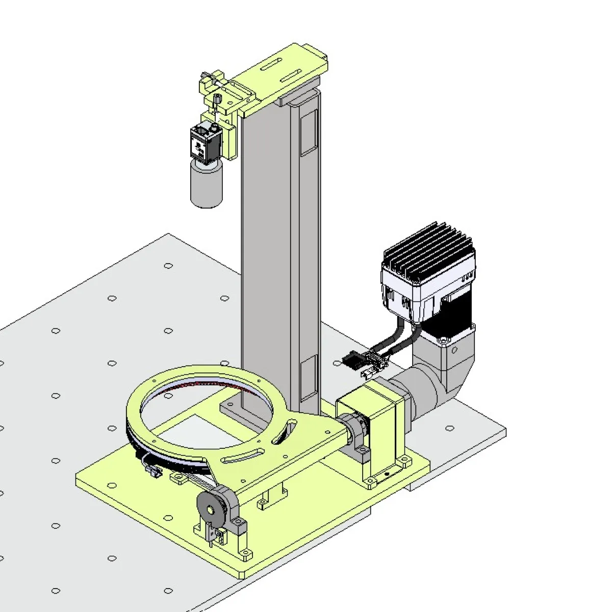
What Does a Vision System Actually Have to Do on an Electronics Line?
A vision inspection system captures an image under controlled lighting, evaluates it against defined criteria, and produces a pass/fail decision or a measurement that the line controller can act on.
| Component | Function | What determines the choice |
|---|---|---|
| Camera | Captures the image, area scan or line scan | Resolution needed, field of view, frame rate |
| Lens | Sets magnification, focus, and depth of field | Working distance, feature size, depth of field |
| Lighting | Makes the feature or defect visible and repeatable | Defect type, surface finish, ambient light |
| Processor and software | Runs the algorithms, stores results, talks to the PLC | Inspection complexity, cycle time, data retention |
The failure point is usually not the camera or the software. It is the lighting, closely followed by part presentation. A defect that is invisible under one lighting configuration is obvious under another, and a part that sits differently in the nest each cycle sets a detection floor no algorithm can beat. This is why we test production parts under several lighting setups before specifying anything.
Which Inspection Tasks Come Up in Electronics Manufacturing?
Component presence, position, and polarity
This is the highest-value and the simplest check on the list. The camera confirms that each component is present, in the right place, and the right way round. Polarity in particular is cheap to catch inline and expensive to catch at functional test.
Lighting is usually diffuse or dome to suppress reflections off component bodies and solder. Resolution is set by the smallest marking you need to resolve.
Connector pin alignment and coplanarity
Bent, missing, or non-coplanar pins are a classic pre-mate failure. Pin position in the image plane is a 2D problem and solves with a backlit or dark-field setup. Coplanarity is a height measurement and needs 3D: laser profiling or structured light.
If the connector mates blind during assembly, this check pays for itself the first time it prevents a damaged mating half.
Dimensional measurement and panel datums
High-resolution cameras with telecentric lenses measure hole positions, gap widths, edge offsets, and datum locations at production speed, feeding statistical process control.
The engineering problem in inline measurement is repeatability across thermal drift, vibration, and part-to-part variation. Measurement stations need thermal compensation, isolated mounting, and a calibration routine an operator can actually run on shift.
Code reading and grading
Reading a Data Matrix code is easy. Grading its print quality is the part that matters for traceability. A grading system evaluates symbol contrast, modulation, decodability, defects, and quiet zone, then assigns a grade under ISO/IEC 15415 for 2D codes or ISO/IEC 15416 for 1D barcodes, and stores that grade with the production record.
Grade the code immediately after it is applied and before the unit is aggregated. A bad code found after aggregation forces you to break the case and reconcile the record. The line-level version of this problem is covered under serialization and traceability lines.
Vision-guided assembly
The camera locates the part or the panel datum and sends a position offset to a robot or servo stage. This removes the need for precise fixturing, because the robot absorbs the placement variation.
On the sensor panel line, the vision system locates panel datums, passes offsets to the SCARA controller, and verifies assembly completion after each operation, holding ±0.01 mm repeat accuracy. The critical procedure is the camera-to-robot calibration: we use multi-point calibration with verification runs so that accuracy holds across the whole working envelope, well past the calibration point. The mechanical side of that cell is described in the SCARA panel assembly case study and in our guide to SCARA robots in electronics assembly.
Keyence or Cognex: Which Platform Fits Your Inspection?
Both platform families are sold widely into electronics manufacturing here, and the choice between them is driven by how variable the defect is. Either one will pass a demo on good parts, so judge them on your reject samples, and on who can support the station at 2 am when the line is down.
| Platform | Strengths | Best fit |
|---|---|---|
| Keyence IV3 | Built-in lighting, fast setup, self-contained | Presence and absence, orientation, simple pass/fail at a single point |
| Keyence CV-X | Multi-camera on one controller, high-speed processing, large tool library | Multi-point inspection, high-speed lines, pattern matching |
| Cognex In-Sight | Spreadsheet programming, AI-based defect classification | Variable or visually complex defects where rule-based logic produces false rejects |
Rule-based tools work when you can describe the defect. When you can only show examples of it, a scratch that matters versus a scratch that does not, a trained classifier will usually beat a threshold. That is the practical dividing line between the two approaches.
Where an application needs non-standard optics or an existing in-house image-processing stack, a generic GigE Vision camera with third-party software is an alternative architecture. It buys flexibility and costs you the integrated toolchain, the vendor support path, and usually several weeks of development.
Compare Cognex and KEYENCE systems on a matched defect set and the functions included in the actual configuration. The 2D vs 3D vision decision concerns the information captured, not the supplier name. The machine vision vs computer vision guide explains the acquisition and machine interfaces surrounding either analysis method.
How Do You Size Camera Resolution for a PCB or a Panel?
Sizing a PCB inspection system starts from the smallest feature you must resolve and works backwards. The arithmetic is simple, and it is where most specifications go wrong.
Resolution at the part = field of view width ÷ sensor width in pixels. You then need enough pixels across the feature: roughly 3 for reliable detection, and 5 or more if you intend to measure it.
| Field of view width | Sensor width | Resolution at the part | Pixels across a 0.1 mm feature |
|---|---|---|---|
| 100 mm | 2448 px (5 MP) | 0.041 mm/px | ~2.4 |
| 100 mm | 4096 px (12 MP) | 0.024 mm/px | ~4.1 |
| 200 mm | 4096 px (12 MP) | 0.049 mm/px | ~2.0 |
| 200 mm | 5472 px (20 MP) | 0.037 mm/px | ~2.7 |
| 400 mm | 5472 px (20 MP) | 0.073 mm/px | ~1.4 |
The bottom row gives about 1.4 pixels across a 0.1 mm feature, below the three-pixel starting point used here. A 400 mm field needs 12,000 horizontal pixels to reach that starting point. Compare higher-resolution area imaging, multiple fields, indexed views and line scan, then verify the choice using actual defect contrast, lens performance, motion and processing time.
Two more constraints that come from the optics: depth of field shrinks as you magnify, so a warped panel can drop out of focus at the edges, and a telecentric lens removes perspective error but restricts you to a field of view no larger than the lens itself.
The machine vision lens selection guide develops the optical side of this calculation, including an object-space sampling example and the limits of treating pixel count as accuracy.
Image acquisition needs a separate hardware check before the inspection sequence is accepted. Compare camera exposure and transfer with the specified feature and motion.
Which Lighting Technique Will Reveal Your Defect?
Lighting is the most critical and most underestimated decision. The same defect can be invisible or obvious depending on angle, type, and colour.
| Technique | Best for | How it works |
|---|---|---|
| Diffuse (dome) | Reflective component bodies, suppressing glare | Light arrives from all angles, minimising specular highlights |
| Directional (bar or ring at an angle) | Surface defects, scratches, texture | Controlled angle casts shadows at defect edges |
| Dark field (low angle) | Fine scratches, raised or engraved features | Near-horizontal light; only defects scatter light back to the camera |
| Backlight | Silhouettes, pin positions, edge measurement | Light behind the part; the camera sees the outline only |
| Structured light | Coplanarity, height, solder paste volume | A projected pattern deforms on the surface; triangulation gives height |
| Coaxial | Flat specular surfaces, wafers, lead frames | Light along the camera axis; specular surfaces return bright |
One practical point specific to electronics: mixed surface finishes in a single field of view, matte substrate, glossy solder, bright metal shielding, often cannot be lit well by one source. Two exposures under different lighting, combined in software, will beat a compromise setup nearly every time.
The lighting trial needs real surface variation and consistent camera settings. The lighting comparison method provides a structured comparison before final equipment selection.
How Do You Present the Board to the Camera the Same Way Every Cycle?
Presentation sets the floor that the camera and the light then work above. A station is repeatable when the board arrives at the same place in the field of view, at the same distance from the lens, and at the same attitude to the light. The last of those is what falls off specifications, because a tilt too small to matter on a drawing moves where a specular highlight lands on a solder joint, and that is a different image for the algorithm to judge.
Board flatness is the electronics version of the problem. A panel carried on its edges sags under its own weight, the sag differs from board to board, and the imaged surface therefore sits at a different point along the optical axis between cycles. Depth of field is what absorbs that movement, which ties the presentation decision back to the optics: magnify harder and the tolerance for sag shrinks. The mechanical answer is to support the board under the area being imaged, and the limit on that answer is the bottom-side components the supports have to miss. That is where a nest stops being a flat plate and becomes tooling with a product name attached to it.
Then decide whether the board stops. Where it stops, the imaging window opens once the mechanics have settled, and never on the motion command completing, so the settle time has to be owned by someone in the cycle budget instead of discovered at commissioning. Where it keeps moving, exposure has to be short enough that the image does not smear, and a shorter exposure is paid for with more light, which sends the question straight back to the lighting table above.
Reference the camera to the datum the downstream operation uses. Where the fixture locates the board on one edge and the robot works from another, the two disagree by whatever the board tolerance allows, and an offset measured from the wrong origin does more damage than no offset at all, because the machine applies it with confidence. A nest under a camera also stays inside the electronics handling chain: the conflict between a fixture that wants insulation and a handling path that wants dissipation is laid out on our wafer handling automation page.
How Do You Size the Station for the Whole Board Family?
Electronics production runs mixes, so a station specified against the board on the bench today has been specified against one member of a family. Two inputs to the sizing arithmetic above can come from different members of it: the field of view has to cover the largest board the station will see, while the resolution requirement comes from the smallest feature anywhere in the family. Where those belong to different products, the worst case of each has to be read together in that table, and the combination is what pushes a single camera into split fields or an indexed sequence.
Sort the specification into what a recipe can change and what it cannot. Reference images, thresholds, tool positions and the check list per variant are recipe. Optics, lighting geometry, the nest and the camera count are not, and a variant that breaks any of those is a rebuilt station presented as a new entry on the HMI.
What a new variant costs, and who absorbs that cost in time, is worth settling before the order. A new recipe needs sample boards of that variant with defective ones among them, and defective samples of a product that has not run yet do not exist. On a board still in introduction the workable sequence is to build the station against the family envelope, accept that the variant on the bench is the one proven at buy-off, and agree in writing which party produces the samples for each later variant and who signs off the recipe built from them.
How Does the Vision System Talk to the PLC and the Robot?
A vision system is a subsystem of a machine. It has to trigger at the right moment, finish inside the cycle time budget, and hand its result to whatever acts on it.
| Integration point | Protocol | What is communicated |
|---|---|---|
| PLC trigger and result | EtherNet/IP or discrete I/O | Trigger, pass/fail, measurement values |
| Robot offset data | TCP/IP socket or a vendor protocol | X, Y, theta offsets for guided alignment |
| MES or SCADA logging | OPC UA or a database write | Images, measurements, statistical summaries |
| Reject mechanism | Discrete I/O from the PLC | Diverter, pusher, or robot sort command |
The control platform is whatever the line already runs, and it matters far less than the split of authority across it. The PLC owns sequencing, safety interlocks, and reject control; the vision system owns image processing. Keeping that split clean is what makes the machine debuggable two years later. Blur it, by letting the camera stop the conveyor directly, and a false reject becomes a line stop with no entry in the PLC fault log to explain it.
Every inspection result should be tied to a part identifier, serial number, panel ID, or a sequence counter, at the moment of inspection. Retrofitting that link is painful, and without it the images you archived are evidence of nothing in particular.
If the inspection uses a learned model, add the AI visual-inspection tests to the sample plan and verify rejection independently of the model result.
What Is the Vision Result Allowed to Decide?
A camera specified for inspection decides quality. It sorts, it measures, it hands an offset to a robot, and it writes a record. It is not the device that makes a hazard safe, and asking it to be one surfaces at safety validation. Whether an opening, an access door or an operator’s reach needs a safety function at all is a risk assessment output under ISO 12100, and where that answer is yes, the function is built from devices rated for the duty. The scope that follows is on our machine safety and CE marking page.
Inside quality the same question is worth asking about authority. A station that only flags is cheap to commission and easy to ignore. A station that stops the line has to be trusted by the shift running it, which makes it a false-reject question before it is a control question, and one to settle with the production supervisor in the room, never with engineering alone.
Where Does the Same Method Apply Outside Electronics?
The sizing, lighting, and integration method above transfers directly to other regulated production. The differences are in what counts as a defect and how much evidence you have to keep.
- Medical devices. Assembly verification and dimensional conformance at each station of a rotary machine, with gauge repeatability studies to prove the measurement system itself. See medical device automation.
- Pharmaceutical packaging. Code grading and label verification tied to a serialization record, on pharma and packaging lines.
What Should You Send Us for a Feasibility Study?
The most productive first step is always a feasibility study with real parts. Nothing else settles the lighting question.
- Sample parts: 5 to 10 good ones, and 5 to 10 with each defect type you care about
- Your current inspection criteria and the tolerances that matter
- Line speed, cycle time, and how the part is presented today
- Existing PLC platform and how the reject mechanism should behave
We test the parts, recommend a configuration, and give you a budget range before you commit. The study either finds a lighting configuration that separates your defect from your good parts, or it establishes that the defect needs a different sensing method entirely, and both answers are worth more than a system that passes a demo and fails on the line. The way we run that study inside a larger build is described in our guide to special purpose machine design, and if you are still comparing suppliers, the system integrator evaluation framework covers what to ask.
Contact the engineering team to arrange a feasibility study, or read more about our work in electronics and semiconductor manufacturing.